 Support Center
Combining Forces
Time of Flight (ToF) technology has been available for industrial use for some years already, however, the release of Sony’s IMX556 DepthSense ToF sensor brings the accuracy and precision of 3D sensing to new levels. With the unique DepthSense pixel structure, Sony’s ToF sensor is able to more reliably reconstruct objects in 3D, in real time, with more detail and with faster frame rates. Coupled with LUCID’s own camera technology Sony’s DepthSense sensor enables maximum potential for industrial use.
How Does Sony's DepthSense IMX556 Time Of Flight Work?
Time of Flight technology works by measuring the time delay of light traveling from a light source, reflecting off a scene, and into a sensor. The specific type of Time of Flight the Sony IMX556 CMOS sensor uses is called continuous wave (CW) modulation, also known as CW phase-shift or Indirect Time of Flight. Instead of measuring the time delay of a single light pulse, the Helios camera emits continuously modulated light, and the phase-shift between this emitted light and the reflected light is used to calculate distance. In order to accurately calculate the phase-shift, the IMX556 utilizes a current assisted photonic demodulator (CAPD) pixel structure that samples incoming light synchronously with emitted light modulation. CAPD allows for an alternating voltage inside each pixel’s photodiode, creating drift fields that divide and pull electrons to alternating detector junctions. In the simplified example below, modulated light is emitted from the VCSEL (Vertical Cavity Surface Emitting Laser) diode. The light is reflected back into the pixel photodiode where it is converted into electrons and divided between the alternating detector junctions. This allows for better light collection efficiency.
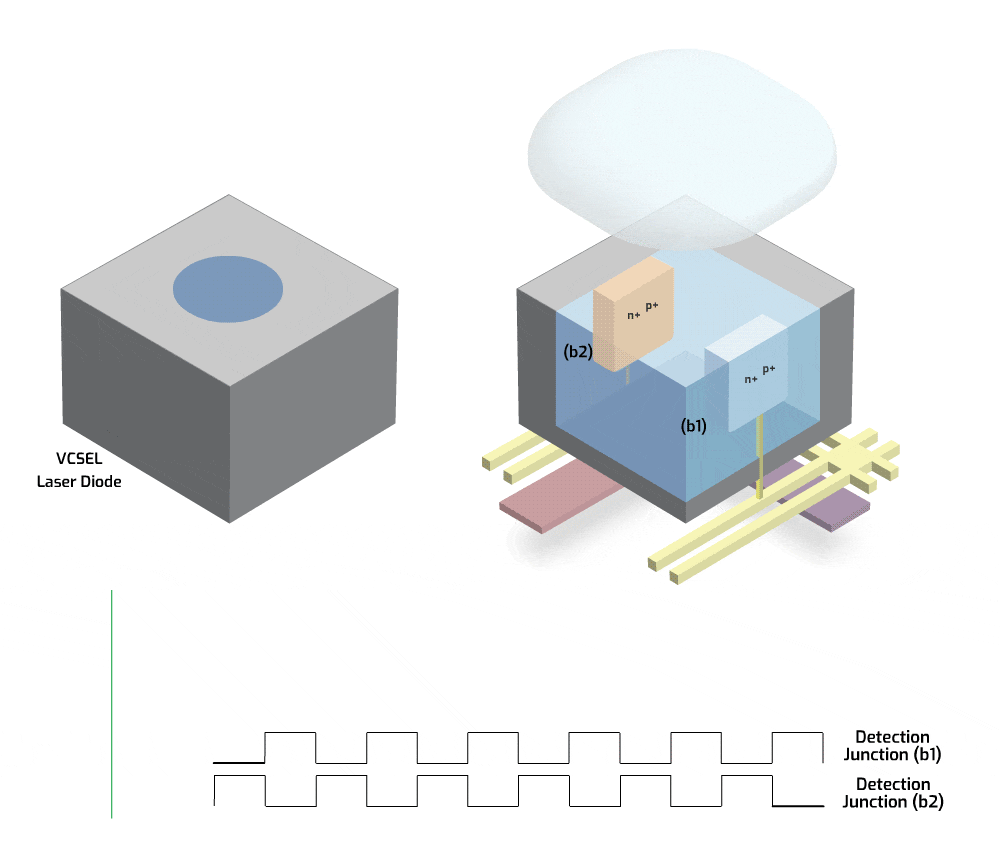
Above: CAPD’s alternating voltage creates an alternating drift field that divides electrons between two detection junctions (b1, b2). This alternating drift field is synchronized to the modulation frequency of the VSCEL laser diodes. The two junctions are 180° out of phase in order to fully capture the reflected light. This is how the sensor can compare the emitted light to the reflected light and calculate the phase shift between the two.
Side Note
Sony IMX556 DepthSense ToF sensor specs:
- Backside Illuminated CMOS
- 640 x 480 px
- Global shutter
- 10.0µm pixel size
- 1/2″ sensor size
Side Note
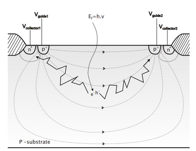
The CAPD ToF image sensor technology was first introduced in 2006 from the founding members of the Belgium based company Softkinetic, acquired by Sony in 2015. Below: CAPD diagram from “Time-of-flight Optical Ranging Sensor Based on a Current Assisted Photonic Demodulator” by D. Van Nieuwenhove, W. Van der Tempel, R. Grootjans and M. Kuijk.
Divide and Conquer
Once the photons are converted to electrons within the photodiode they must quickly be pulled towards the detector junctions for the camera to accurately calculate the phase shift. Located in each detection junction are positive (p+) and negative regions (n+). When a current is introduced to produce a drift field, the electron holes (h+) move towards the lowest voltage p+ region and the electrons (e-) move in the opposite direction towards the highest voltage region (n+). CAPD is extremely fast and effective. It is able to quickly alternate drift field polarity producing very high demodulating contrast. A high contrast ratio means more electrons are directed to the right junction based on their return time, allowing for higher quality phase shift calculations. This results in better accuracy and precision with the DepthSense sensor. In addition, CAPD’s drift field is able to reach deep into the photodiode accelerating as many electrons as possible towards the detection junction. This, combined with Sony’s backsided technology helps produce a high quantum efficiency of 57% at 850 nm. As a result, the Helios camera can achieve an accuracy of less than 5 mm and a precision of less than 2 mm at 1 m camera distance.
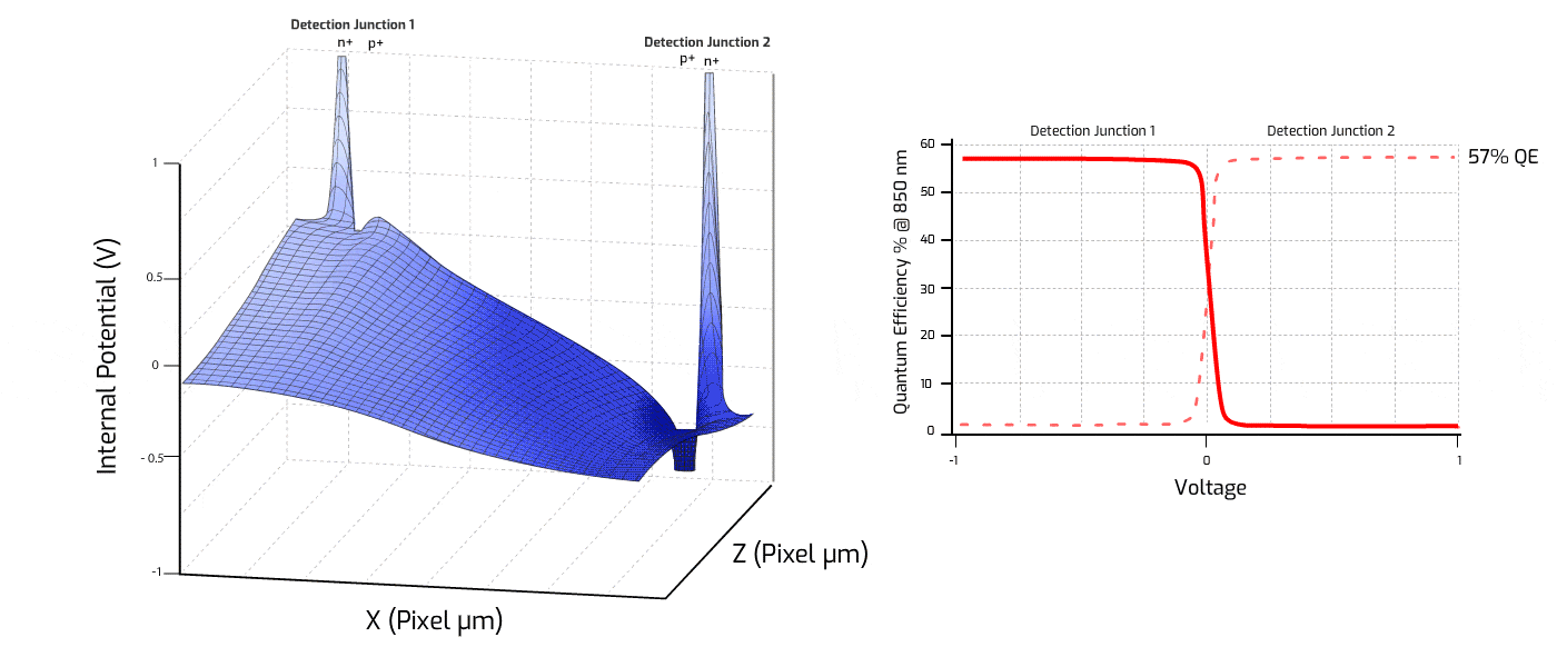
Above Left: Cross-section of a CAPD’ showing electrons (e-) accelerating towards the highest voltage region (n+) while the electron holes (h+) move towards the lowest voltage region (p+) Above Right: CAPD helps produce high QE (57% at 850nm) and high demodulation contrast.
1 Frame, 4 Phases
The speed of CAPD allows the IMX556 to sample incoming light with 4 different phases for each depth frame. Each sample, also known as a micro-frame, is phase-stepped by 90° (0°, 90°, 180°, 270°) with each one having 3 stages: reset, integration, and readout. During the reset stage, the pixel voltage is reset back to baseline. The Integration stage occurs when the drift-fields are introduced by the current to direct the electrons towards the detection junctions. During the readout stage all pixel data is read on the sensor. After the readout stage the sensor enters idle time to reduce power and lower heat levels.

It is only necessary to have the 0° and 90° micro-frames to calculate depth. As the distance of an object changes, the values of b1 and b2 in the 0° and 90° micro-frames will change. Ambient light is also easily removed by subtracting the values of b2 from b1. However, even if the collected photons are the same for b1 and b2, there are always slight fluctuations (caused during photon to electron conversion and electron to voltage conversion). It is important to cancel out these fluctuations and their influence on b1 and b2 values. By having 2 additional micro-frames that are 180° offset from 0° and 90° (which effectively reverses the roles of b1 and b2) and by adding the values of b1 and b2 to their opposite 180° micro-frame (and vis-versa) the camera cancels out these fluctuations in each pixel.

Subtracting b2 from b1 cancels out the ambient light in each micro-frame.
Adding b1 of the 0° micro-frame to b2 of the 180° micro-frame (and vis-versa) gives two new quantities that are free of any sensitivity discrepancies in b1 and b2 (discrepancies that are caused during conversion stages such as dark offset, gain, etc.)
CAPD + Backside Illuminated CMOS
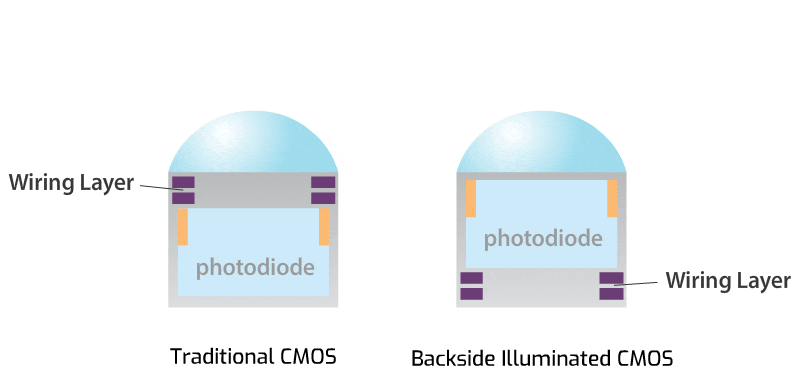
CAPD provides an effective way of demodulating and collecting electrons inside the photodiode, but reflected light must first reach the sensor’s photodiode unobstructed. Sony’s backside illuminated (BSI) technology ensures the maximum amount of light reaches the photodiode. Unlike traditional front-side CMOS sensor design, backside illuminated sensors place the wiring layer below the photodiode improving light sensitivity. This placement removes any wiring or circuit obstructions that might otherwise block some of the incoming light.
Reducing unwanted image artifacts is another benefit of the IMX556. Because the IMX556 is a CMOS sensor it performs better against smearing and blooming versus CCD ToF sensors. Smearing and blooming can cause erroneous 3D data and is created when the charge overflows the pixel well capacity, spilling into adjacent pixels. This is usually caused by intense light sources or reflective surfaces. In many ToF use cases, it is important to minimize these factors. The IMX556 CMOS used in the Helios camera is much more forgiving in reducing these image artifacts.
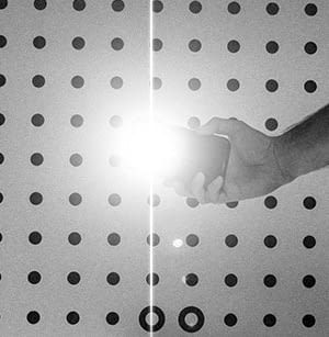
Above: CCD blooming and smearing artifacts
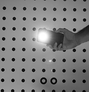
Above: CMOS image without smearing and less blooming
VCSELs: High Performance Light
The emitted light used for distance calculations is critically important to the performance of a ToF camera. To ensure reliable performance the Helios camera uses 4 vertical cavity surface emitting lasers (VCSEL) to emit modulated light. The VCSELs emit a tailored beam shape of narrow-band light at 850nm with high peak power and fast rise and fall times. Besides producing high modulation contrast, the narrow emission band at 850nm does not emit any visible spectrum (380 to 740nm) light that might interfere with other 2D cameras in the system. Unlike edge emitting lasers, VCSELs have lower coherence which results in speckle-free images. Higher peak power illuminates the scene with more photons resulting in less noise and better immunity to ambient light to produce better precision in distance calculations.

Above: The Helios VCSELs emit enough light at a narrow wavelength of 850nm to take advantage of the 56.6% quantum efficiency (at 850nm) of the IMX556 CMOS sensor.
Side Note
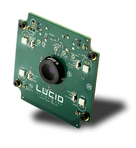
The Helios ToF camera uses 4 VCSELs mounted to the front of the camera. The VCSELs are the small white squares located near each corner of the imager board.
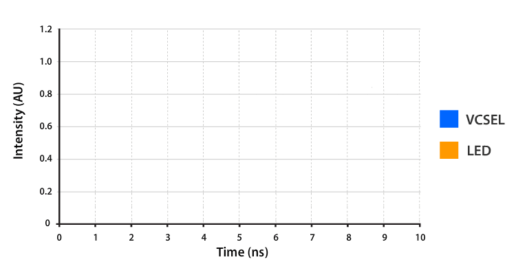
Above: VCSELs have faster rise and fall times compared to LEDs, which makes them excellent light emitters for CW phase-shift ToF sensors such as the IMX556. The VCSELs can also produce high modulation frequencies for better accuracy and precision for shorter distances.
Conclusion
Sony’s IMX556 DepthSense ToF sensor enables reliable, accurate, and precise 3D measurements. The combination of the innovative CAPD drift field technology combined with Sony’s expertise in back-illuminated CMOS makes the DepthSense sensor an excellent choice for industrial camera integration. Additionally, LUCID’s Helios camera featuring the IMX556 sensor offers users an industrial strength camera with high contrast scene illumination from it’s 4 VCSEL emitters. While there are other ToF solutions currently available, the most viable for industrial use is the Helios camera, enabling the IMX556 to reach an accuracy of less that 5mm (0.3m to 1.5m camera to object distance) and a precision of less than 2mm at 1m distance.
Helios2, Helios2+, Helios2 Wide, Helios2 Ray ToF Cameras featuring Sony DepthSense Sensor
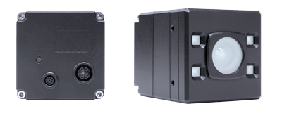
Helios2 Time of Flight 3D camera models.
The Helios2 models are 3D, high precision ToF cameras with four 850nm or 940nm VCSEL laser diodes and integrates Sony’s new DepthSense™ IMX556PLR back-illuminated ToF image sensor. The camera delivers 640 x 480 depth resolution with up to 8.3m working distance. On-camera processing provides range, intensity and confidence data which reduces the need for expensive host systems components. IP67, shock and vibration certified, EMC industrial immunity, and M12 Ethernet connection makes the camera ideal for factory and warehouse environments. Visit the Helios2 Product Page